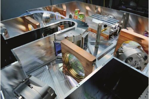
By harnessing the power of a 20 kW laser, their laser-diode floating zone (LDFZ) method eliminates the need for conventional crucibles, resulting in larger, purer crystals vital for electric cars and photovoltaics.

German and Japanese researchers have advanced semiconductor crystal production, which is essential for applications in electric cars and photovoltaics. The team, comprising scientists from the Fraunhofer Institute for Laser Technology ILT in Aachen and the National Institute of Advanced Industrial Science and Technology (AIST) in Tsukuba Science City, has developed a method for producing high-purity semiconductor crystals using a laser-based process, eliminating the need for a crucible.
This technique, known as laser-diode floating zone (LDFZ), utilizes a powerful 20 kW laser and a process-adapted optical system developed by the Fraunhofer ILT team. Unlike traditional methods reliant on crucibles, the LDFZ process minimizes crystal contamination by directly supplying heat via radiation, resulting in the remelting of polycrystalline material into high-purity single crystals.
The advantages of this approach are manifold. The precise control afforded by the laser beam’s directionality and stability ensures targeted and efficient heat input, producing larger, purer semiconductor crystals. Moreover, the meticulously designed and water-cooled optical system to withstand the high laser powers facilitates even crystal heating during growth.
With the new 20 kW system, the researchers aim to increase crystal diameter significantly. Initial experiments have yielded promising results, with crystals up to 30 mm in diameter successfully grown—the largest ever produced using a crucible-free method. Detailed findings from these investigations are forthcoming and are expected to contribute significantly to the field of semiconductor crystal production.
Dr. Martin Traub, project manager at Fraunhofer ILT, expressed satisfaction with successfully commissioning the system, noting the novel use of video conferencing for installation and testing amid pandemic restrictions. The team highlighted the potential of the LDFZ process, having already produced gallium oxide crystals with a diameter of up to 12 mm at lower laser powers. This collaborative effort represents a significant milestone in semiconductor technology, paving the way for enhanced performance and efficiency in power electronics for electric vehicles and renewable energy systems.
The post Laser-Based Method Revolutionizes Semiconductor Crystal Production appeared first on Electronics For You.